‘Zero conviction in 152 paper leaks’: Rahul Gandhi says India’s education system ‘rigged’ under current dispensation
Rahul Gandhi has alleged that the education system has been “rigged” under the current dispensation.
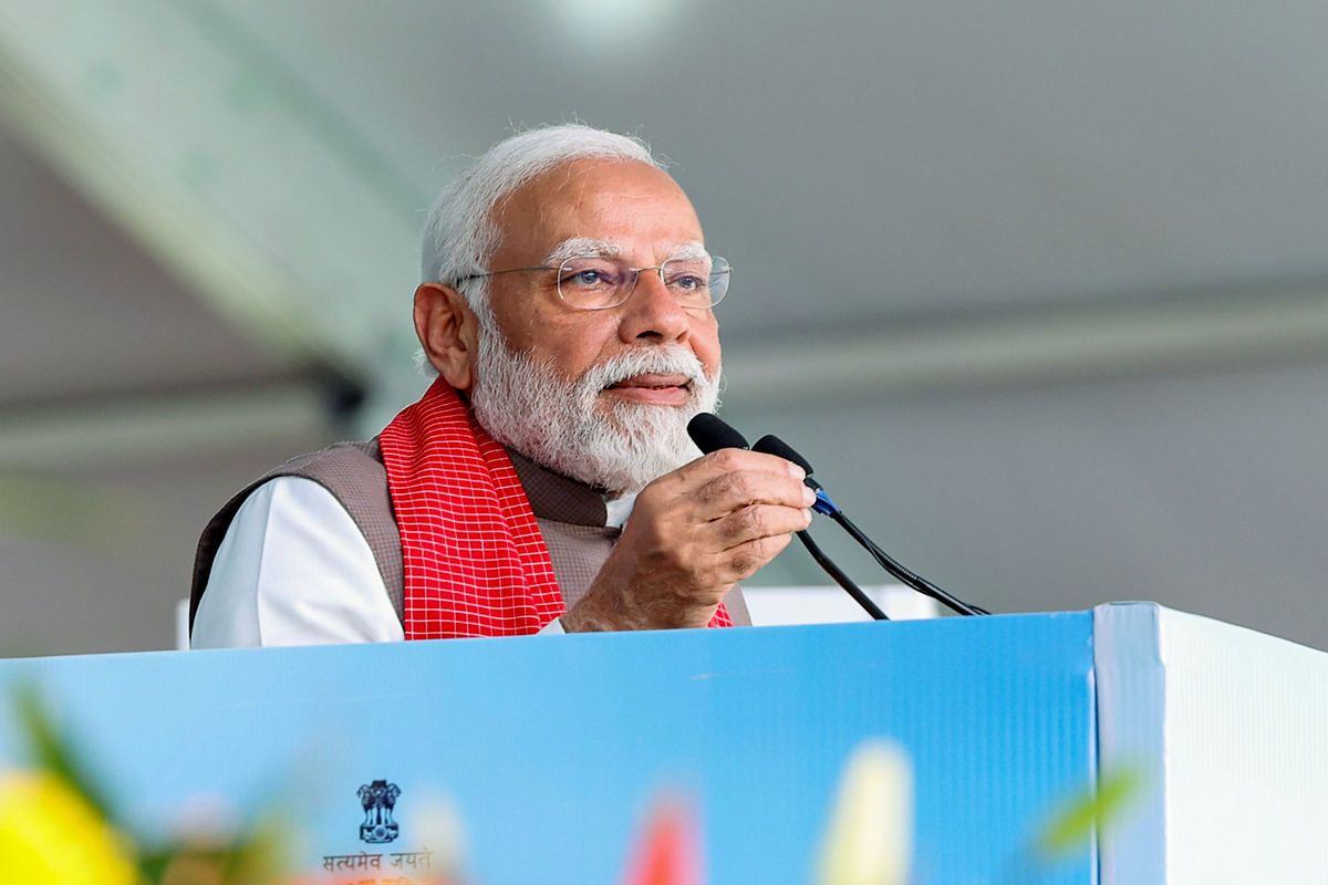
The Prime Minister decided to position India as a global hub for semiconductor design, manufacturing and technology development, fostering the creation of employment opportunities for the nation’s youth.

PM to lay foundation stones for Rs 1.25 lakh cr semiconductors projects
Prime Minister Narendra Modi will participate in ‘India’s Techade: Chips for Viksit Bharat’ and lay the foundation stone of three semiconductor projects worth about Rs 1.25 lakh crore on Wednesday via video conferencing. He will also address the youth across the country on the occasion.
The Prime Minister decided to position India as a global hub for semiconductor design, manufacturing and technology development, fostering the creation of employment opportunities for the nation’s youth.
Advertisement
In line with this vision, foundation stone is being laid for the semiconductor fabrication facility at the Dholera Special Investment Region (DSIR), Gujarat; Outsourced Semiconductor Assembly and Test (OSAT) facility at Morigaon, Assam; and the Outsourced Semiconductor Assembly and Test (OSAT) facility at Sanand, Gujarat.
Advertisement
The semiconductor fabrication facility at the Dholera Special Investment Region (DSIR) will be set up by Tata Electronics Private Limited (TEPL) under the modified scheme for setting up of Semiconductor Fabs in India. With a total investment of over Rs 91,000 crore, this will be the first commercial semiconductor fab in the country.
The Outsourced Semiconductor Assembly and Test (OSAT) facility in Morigaon, Assam will also be set up by Tata Electronics Private Limited (TEPL) under the Modified Scheme for Semiconductor Assembly, Testing, Marking and Packaging (ATMP), and with total investment of about Rs 27,000 crore.
The Outsourced Semiconductor Assembly and Test (OSAT) facility in Sanand, will be set up by CG Power and Industrial Solutions Limited under the Modified Scheme for Semiconductor Assembly, Testing, Marking and Packaging (ATMP), and with total investment of about Rs 7,500 crore.
Through these facilities, the semiconductor ecosystem will be strengthened and will get a firm footing in India. These units will also provide employment to thousands of youth in the semiconductor industry as well as catalyse employment generation in related sectors like electronics, telecom etc.
The programme will witness massive participation of youngsters including thousands of college students, along with leaders from the Semiconductor Industry.
Advertisement